Why this key chip technology is crucial to the AI race between the US and China
In a landmark move, Taiwan Semiconductor Manufacturing Company (TSMC) has announced an unprecedented $100 billion investment, marking the largest single foreign investment in U.S. history. This significant financial commitment has captured global attention and stirred concerns within Taiwan itself. TSMC, responsible for producing over 90% of the world’s advanced semiconductor chips—which power a range of technologies from smartphones to artificial intelligence (AI) systems and even military applications—plans to establish two new advanced packaging facilities in Arizona, among other locations. The surge in demand for advanced packaging technology has paralleled the global AI boom, making it a focal point in the ongoing rivalry between the United States and China for dominance in AI. Although both nations have recently agreed to a temporary truce that suspends disruptive tariffs for 90 days, tensions remain high due to ongoing disputes over chip restrictions and other geopolitical issues. At Computex, a prominent trade show in Taipei that has gained prominence due to the AI frenzy, Nvidia's CEO Jensen Huang emphasized the critical importance of advanced packaging for AI development, stating, "No one has pushed advanced packaging harder than me." This technology refers to the manufacturing process of semiconductor chips, specifically the methods used to encapsulate chips within protective casings and integrate them into the electronic devices they power. Advanced packaging techniques allow for multiple chips—such as GPUs, CPUs, or high bandwidth memory—to be positioned closer together, resulting in enhanced performance, quicker data transmission, and reduced energy consumption. Dan Nystedt, vice president of a private investment firm, likened this arrangement to departments within a company: the closer they are, the more efficient the operation. This innovation plays a pivotal role in upholding Moore’s Law, which suggests that the number of transistors on microchips doubles approximately every two years, despite the rising costs and complexities of chip fabrication. TSMC's CoWoS (Chips-on-Wafer-on-Substrate) technology has become particularly notable since the AI boom ignited by OpenAI's ChatGPT. CoWoS has become a household term in Taiwan, as emphasized by AMD's CEO Lisa Su, who noted that people in Taiwan readily recognize the term. This advanced packaging is crucial for ensuring that complex AI applications run smoothly and without interruption, making it essential for producing AI processors, particularly Nvidia and AMD GPUs used in data centers. As demand for CoWoS technology skyrockets, TSMC is working to increase its production capacity. During a visit to Taiwan, Huang revealed that the current capacity for advanced packaging has increased significantly over the past two years. He highlighted the importance of sophisticated packaging solutions for the future of computing, stressing the need to integrate multiple chips into single, powerful units. Having advanced packaging capabilities alongside chip fabrication in Arizona positions the U.S. as a formidable player in the semiconductor supply chain. This strategic development is expected to benefit major tech companies such as Apple, Nvidia, AMD, Qualcomm, and Broadcom. According to Eric Chen, an analyst, this arrangement not only strengthens the U.S. competitiveness in AI chips but also minimizes potential supply chain risks by diversifying production locations. Although CoWoS technology has existed for over 15 years, it was initially met with skepticism due to high costs. Its creator, Chiang Shang-yi, faced significant pressure during its early development stages. However, the recent AI surge has transformed CoWoS into a sought-after technology, exceeding initial expectations. The global semiconductor landscape includes various firms specializing in packaging and testing, with TSMC, Samsung, and Intel being key players in advanced packaging technologies.
Sriram Krishnan Bids Farewell as AI Advisor to the White House
Sriram Krishnan, a prominent figure in the tech industry and venture capital, is stepping down from his position as a se...
TechCrunch | Jun 06, 2026, 18:10
Meet Jay Hoag: The Venture Capitalist Ready to Lead Netflix into a New Era
Replacing a figure as iconic as Reed Hastings is no small feat, yet Jay Hoag is set to take on this monumental challenge...
Business Today | Jun 06, 2026, 06:45
Revolutionizing Air Travel: Inside Beta Technologies' Groundbreaking Alia CX300
The Alia CX300, an innovative electric aircraft by Vermont-based startup Beta Technologies, is set to redefine the futur...
Business Insider | Jun 06, 2026, 08:25Apple's Upcoming MacBook Ultra: A Game-Changer with OLED Displays and New Sizes
Apple is gearing up to launch its highly anticipated MacBook Ultra, a premium laptop expected to surpass the existing Pr...
Business Today | Jun 07, 2026, 05:55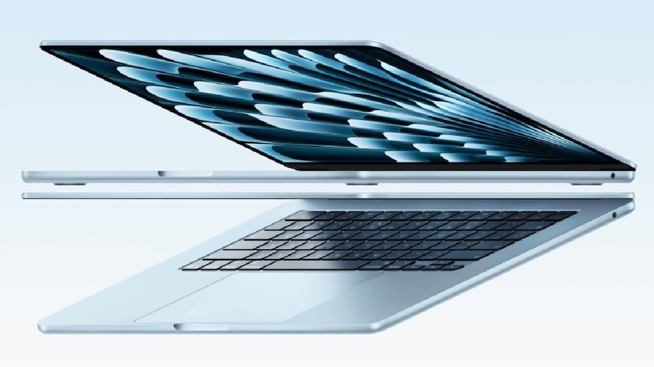
Five Scientists Expelled from Diabetes Conference Over Controversial Editorial Distribution
In an unexpected turn of events, five prominent scientists were removed from the American Diabetes Association's (ADA) a...
Ars Technica | Jun 06, 2026, 20:55